8th August 2020
Been a bit of a busy week at work so I'm only just finishing off the PCB panel at the moment. I did wire up a prototype during the week, and test with the new CPLD code (I'd moved a few pins around, and reused the JTAG pins as IO to free up a few more pins on the device for possible future updates/flash optimisation).
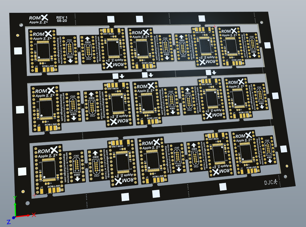
This is the panel layout that I'll be using:

The main reason why I want to put the boards on a panel (versus individually routed boards) is to reduce the assembly time. A solder paste stencil can be ordered with the boards - solder paste is applied to the panel with a squeegee, leaving solder paste only on the areas exposed by the stencil (the component pads). The parts can then be placed either by hand, or by pick-and-place machine onto the panel. Once placed, the panel is put into an SMD reflow oven where it is heated (following a specific reflow temperature profile) - the solder paste will melt, soldering the parts onto the panel. When cooled, I can repeat the process with the parts on the other side of the panel. The end result is that 15 ROM X boards can be done at a time, relatively quickly. A lot faster than hand soldering them! Of course there is still the hand soldering of the headers and pins, but a fair amount of time will saved by semi-automating the soldering of the other components.
The ROM X panel layout is based on my cosmetic requirements for the final boards that will be shipped. Since there is no enclosure to hide the PCB, I wanted it to look as presentable as possible. Clean edges, with a minimum number of mouse bites or other breakaway areas visible on the final boards (mouse bites are the drill patterns where you want the board to snap away from a tab - it will generally leave a bit of a rough edge that looks a little like a mouse has been chewing on it!). Originally I was going to go with a panel of 5 x 5 boards, but that meant that there would be up to 4 mouse bites on each final board. I also considered a combination of v-scoring and tab routing, as that would offer the greatest yield per panel size. V-scoring (where the boards are scored in a V shape 1/3 of the way through on each side leaving 1/3rd of the thickness along which the boards are snapped) also leaves a slightly rough edge though, whereas the routing leaves a very clean edge.
With the layout above, one of the mouse bites is behind the ROM-Link header, leaving only one other on the right edge of the PCB - a reasonable tradeoff. This did mean a lot of wasted PCB area as I needed to include the horizontal strips. One has to also keep in mind that the panel needs to be strong enough to be routed out without breakaway of any of the nested PCB's during manufacture, needs to be strong enough to not flex too much on a stencil printer or pick-and-place machine, plus one also needs to think about de-panelisation - breaking out the individual boards after soldering has been completed. This needs to be done in such a way that minimal forces are applied to parts on the board. In my case I've drilled the frame in a number of locations such that I'll be able to firstly snap the panel along the line of holes on the frame, and then snap out the individual boards via the mouse bite behind the ROM-Link header.
There also needs to be tooling holes on the panel where it will be held in a stencil printer (or suitable tooling block that is used to align the solder paste stencil), and possibly fiducual marks (usually 3) for a pick-and-place machine to be able to optically align itself to the panel. The tooling holes may also be required to fit the board into a pick and place machine, depending on the machine. In this example, 4 x 2.5mm tooling holes are used to suit the stencil equipment that I have available. I've also put fiducials on the panel, so I can run the boards through the pick-and-place machine at my workplace if I want to (else I'll just hand place them as there aren't that many to place).
Lastly, I've included some check boxes on the frame which can be used during inspection after soldering - to mark any board where re-work may be required (such as a removing a solder bridge between pins etc).
I'm pretty happy with this layout and hope to send off the manufacturing files in the next day or two. They may request changes to the layout to add additional strength, but I think I'll be ok with this one -we'll see!
