21st August 2020
After a few delays (I have been quite busy with my normal day job!) all the PCB's are on order. This includes a number of other boards that I've designed to assist with assembly and production programming of both the ROM X and the ROM X 2316B SPCL PCB.
First of these is an adapter for the ROM X board - to allow programming/dumping of the flash chip in an EPROM programmer, but also to assist with re-programming of the CPLD if required .
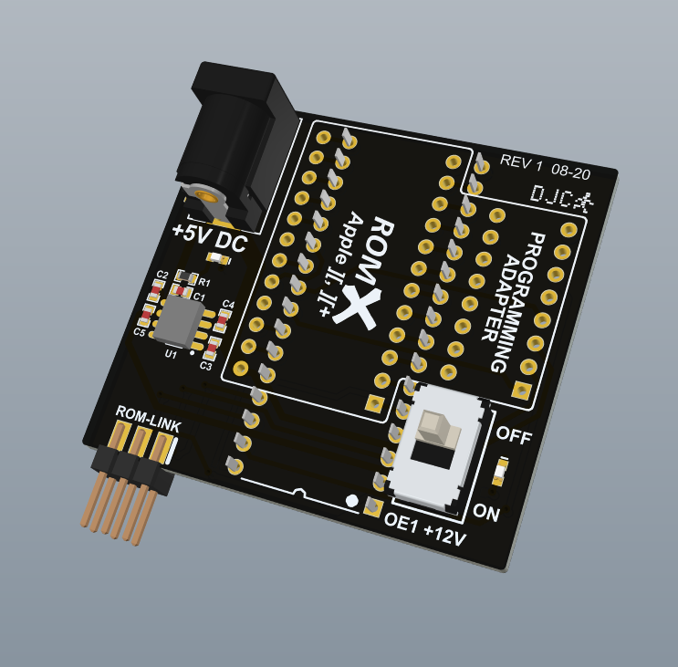
Whilst the end user will program ROM X in-system, I need to be able to get the initial firmware image onto the flash to begin with.
I do have a TSOP adapter for my EPROM programmer which would allow me to pre-program the flash chips before they are soldered down, but this ROM X adapter PCB will be useful when setting up the production flash image. When the base image is spot on, I'll be able to easily take a backup copy. The copy will then be used to pre-program the rest of the flash chips.
You may be wondering why it has a 5V DC jack on it. I've found that my EPROM programmer can't provide enough current to power the CPLD as well as the flash chip - thus this adapter removes the power requirement from the EPROM programmer - all power is supplied via the 5V DC Jack.
You'll also probably be wondering why what should be a simple socket adapter has a chip on it. The chip is a DC-DC charge pump to produce +12V from the +5V DC input. The +12V is linked via the switch to the OE1 input on the CPLD. The production version of the ROM X board re-uses most of the JTAG pins for IO. Thus, when programmed, the JTAG is no longer available. There is a trick though - if you can safely apply +12V to the OE1 pin on the CPLD then you can re-enable the JTAG port.
So this adapter gives me that functionality if I need to re-program the CPLD for any reason. Flipping the switch to the ON position disconnects the OE1 CPLD pin from the EPROM programmer (pushing +12V back into the EPROM programmer is not a good idea) and connects it to +12V, after which I can connect the JTAG adapter and erase the CPLD. After erase, the JTAG port is re-enabled and the CPLD can be re-programmed. I've included an LED on the +5V DC input to show that the board is powered, and also on the +12V output where the LED will light when the switch is in the ON position.
The next adapter is a much simpler one - an adapter to allow re-programming of the flash chip on the 2316B SPCL board in an EPROM programmer :
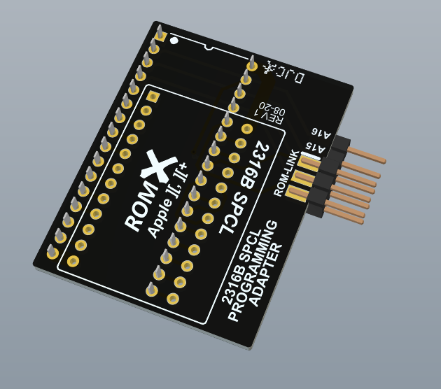
Not much more to say on that one - again it allows me to tweak the image and copy it off for produciton.
Lastly I did an assembly jig that is made up of 7 PCB's soldered together (3 different board designs) :
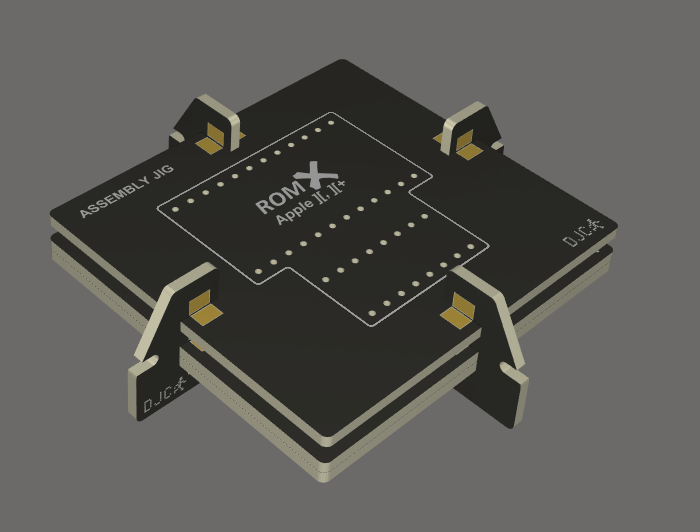
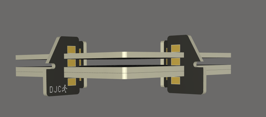
The jig is to assist in fitting the pin headers to the ROM X and ROM X 2316B SPCL boards. It aligns the pin headers vertically using the topmost 2 boards which have unplated drill holes in them, plus it sets the pin length as the bottom board in the stack has no holes. The pin headers pass through the ROM X board, then the top two boards on the jig, and stop at the bottom board on the jig. I can then solder them in place, snip off the excess, and remove the ROM X board which should now have near perfectly aligned headers installed.
Unplated holes is important on a jig like this - the last thing you want is solder flowing down through the ROM X board, and sticking to your assembly jig - joining the two together!
With the panels for ROM X (here) and ROM X 2316B SPCL (here) I also ordered the solder paste stencils. Hopefully we will be shipping ROM X boards out very soon :)
