31st July 2020
I'm just finalising some changes to the board for the production version - changes that are primarily centered around the recovery mode.
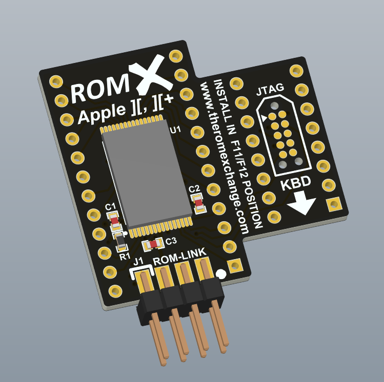
I've added a jumper J1 at the end of the ROM-Link header (I'll likely have to space that out a little more so that a jumper will fit alongside the header before I submit the design). J1 will be used to select recovery mode should your main firmware image be corrupted whilst updating it (power outage mid cycle for example).

For normal operation a jumper would be installed in the J1 position whilst the 6 way ribbon cable to the (optional) ROM X character ROM board would be installed on the ROM-Link pins. If the firmware is corrupted, power off, remove J1 and power the machine back on - a recovery menu will be displayed allowing you to boot from ROM image 1 through F. Once booted, you can load the disk version of the firmware, and re-flash the firmware onto the device. The chances of you not having at least one working ROM image loaded should be low - the boards will ship with all 15 slots containing working images.
You'll note that the production header for the CPLD is shown on this board. The CPLD programming is a once off thing at time of manufacture thus I've opted for a Tag-Connect header. The Tag-Connect header has no physical part - just pads and alignment holes. The programming cable has 3 guide pins which locate it in the correct orientation on the PCB (they pass through the 3 alignment holes on the board) plus 10 pogo pins for the JTAG interface (pogo pins are sprung pins - to maintain electrical contact on the pads) . Press the header to the board, program the CPLD, and pull the header away. Once programmed, the header will not be used again (unless you send the board back for some future update or something along those lines).
Jeff is working on the recovery software at present.
Next step is to update the CPLD code to match this layout (the changes required some pin remapping on the CPLD to keep the layout clean), load the recovery image into flash, and test it before laying out a production PCB panel. The PCB panel will be a matrix of these boards - maybe 5 x 5 so I can populate then reflow solder 25 at once!
